
By Joseph Birtola
The clock is ticking, and your management is all over you to get rolling on your new PCB design! No problem, you got this! You will just send your design engineer a few blurbs about the layout and get back to other tasks! “Hi, Mr. Layout Designer, I have a new PCB design that I would like you to get started on. Attached are the RFQ, POD, DUT and BOM. I need boards by next Friday. I’m going on vacation now. Please get started!”.
Pretty cool, you described the entire project in 12 letters’ worth of acronyms! And though those documents will lend a ballpark vision of the scope of work, expect the design engineer to come back to you with many questions, or worse… big-time ERRORS! Though this seems like an extreme example, I’ve experienced first-hand this real-case scenario!

After seeing decades’ worth of design input packages, we have seen the good, the bad, and the very ugly of PCB design package submissions. There is a term in the layout business… “garbage in, garbage out” that every PCB design “customer” should keep in mind when preparing their project information. The truth is, more than half of the input packages we see come into us incomplete, lacking circuit performance requirements, incomplete component part numbers, and large holes in the overall spec. Dare I say “Napkin drawings”? Oh, it still happens, and I find it charming as it brings me back to those early days of layout!
It’s ok!
We get it, resources are thin, time is short, and you need a board yesterday! Perhaps PCB layout and development is not exactly your strong suit. Maybe you know just enough about DFM to be dangerous. Or maybe you’re just looking for a little help from your supplier because you are overwhelmed with the process. It’s very common… We are not here to scold you; we are here to help.
Though design engineers know a lot about board design, they are not mind-readers and your input should be built on this premise. It is understood that not everybody has the time to create a formal written outline with embedded photo image samples. We do see these types of submissions from time to time, and they are wonderful, organized, and easy to follow. However, in most cases, a detailed email with attachments will do just fine. It’s the content that matters most. Below are some examples of what to consider when compiling your design input package for the design engineer:
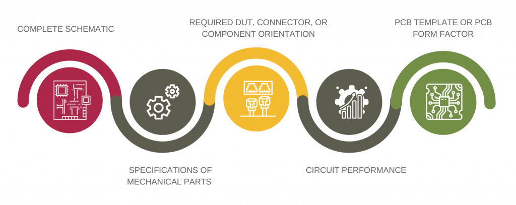
Complete Schematic – Will you be the author of the schematic? If so, be sure it is complete, or advise your design engineer if there are items that you would like to have him/her finish up for you. If you will have the design engineer capture the schematic, be sure to provide full part numbers or full value/spec. requirements of components that you will require to be used. Provide a complete connection list and any required circuitry in a format that is easy to read and understand. Include notes as to special handling of select nets when applicable. Solid guidance here will help the process be efficient and minimize the risk of error.
Specifications of Mechanical Parts – Provide a list and specifications of mechanical parts that will be in play. Are drawings available? Note how these items may affect the PCB layout. Will these items create via, component, and signal keep-out areas on the PCB that are not obvious? Mounting brackets, cooling fans, heat sinks, EMS shields, probe station PCB rails, and handler docking plates would be examples of mechanicals that require such consideration.
Required DUT, connector, or component orientation – What side of the board do critical parts reside on? These get left out of the input package quite a bit. But it will always stop a design engineer in their tracks if they don’t have the information on hand. Also, if a required orientation of the part is not given, a design engineer may assume that the orientation is at their discretion since a preference was not given. Rotating parts after a layout is complete, can be disastrous! If there are no part orientation requirements, then it is always good practice to state that upfront. It will head off a lot of questions.
Circuit Performance – A design engineer is unlikely to know about your signal performance needs just by looking at a schematic. Communicate your required performance and signal characteristics to the design engineer for items such as high-speed data rates, impedance control, phase matching, and coupling for differential pairs. Current/voltage for power supplies should be noted. After review and consultation with the design engineer, it may be determined that circuit simulations are required to assure the best result.
PCB template or PCB Form Factor – Be sure to include specifics of the PCB template or PCB form factor required. For ATE Test, for which tester manufacturer and model will this PCB be used? What is the tester configuration? The layout engineer will need to validate that his/her template coincides with the required resource requirements and where they are located on the board vs. the tester. Identify required positioning for any fixed interface mechanicals or connector locations.
These are just some examples of the information and the approach, that will prove to go a long way in promoting a streamlined, on-schedule, high-quality PCB layout that stays within budget. Your upcoming layout will likely have other features and requirements that you will want to convey. Hopefully, the information within this article will get you thinking about how you can best help your design engineer in the development of your printed circuit board… and find that all it took was to provide a great design input package!